Evaluator ASIC Design
- 👋 Supranational
Verifiable Delay Function Evaluation ASIC
Introduction
The VDF ASIC is a fixed function device that takes a message hash, difficulty level, and interval then returns the VDF result at each interval. The intended usage is part of Ethereum 2.0’s transformation, a cornerstone in several of Filecoin’s core components, as well as other blockchains initiatives.
Verifiable Delay Function
The Verifiable Delay Function (VDF) used in the ASIC is based on the work of Benjamin Wesolowski: Efficient verifiable delay functions
The VDF result ![]() is generated by the following formula with the input hash
is generated by the following formula with the input hash ![]() and difficulty
and difficulty ![]() :
:
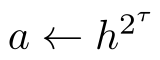
Typically ![]() will be on the order of 240.
will be on the order of 240.
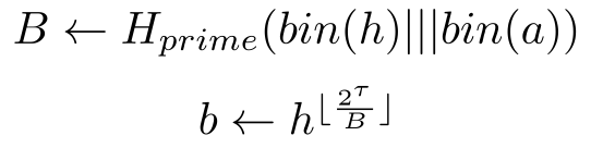
The proof is calculated by:
For more information on VDF’s refer to the project research page: VDF Research
Requirements
Input Bandwidth | TODO – small - < 10KB per job depending on precomputed constants |
Output Bandwidth | TODO – little bigger, still small - < 2Mbps |
Power | TODO – depends on system ~10W? |
Mod Square Latency | TODO – 2 ns? |
Thermal | TODO – 0-100 C |
IO Voltage | TODO – 0.8 V |
Logic Voltage | TODO – 0.75 V |
PLL Reference | TODO – 25 MHz |
ASIC Overview
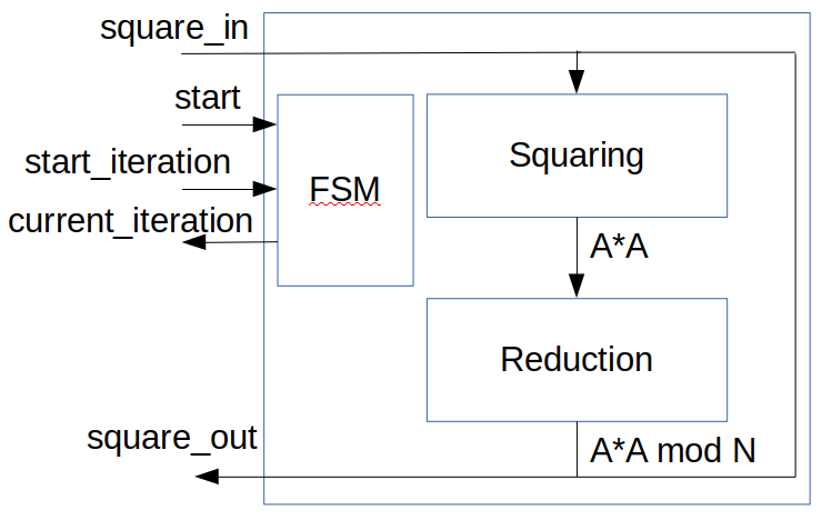
There are five main blocks in the VDF ASIC: Modular Squaring Unit, Input/Output Logic, Control Logic, PLL, and Thermal Sensor.
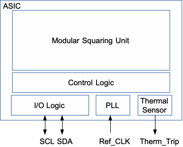
Modular Squaring Unit
The Modular Squaring Unit (MSU) is the primary compute engine in the VDF ASIC. The engine takes a 2048 bit input ![]() and returns
and returns 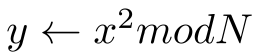 where
where ![]() is a predefined 2048 RSA modulus. There is a built-in feedback loop that continuously takes the output of the current result as the input to next. This is required for the iterative modular squaring of the VDF evaluation function.
is a predefined 2048 RSA modulus. There is a built-in feedback loop that continuously takes the output of the current result as the input to next. This is required for the iterative modular squaring of the VDF evaluation function.
The MSU has control logic around the compute engine to keep track of the current iteration and optionally return intermediate values for use in proof generation. Note the proof generation aspect of VDFs is not applicable in this ASIC.
Input/Output Interface
Given the small volume of data that goes in and out of the ASIC, I2C is used as the low speed I/O protocol. The benefits of I2C are being well known, robust, and very simple. Alternatively there are options to go with SPI, UART, or a non-standardized basic serial interface if necessary.
For details on I2C, please refer to the user guide from NXP.
The ASIC is configured as an I2C slave and is not required to be fully I2C protocol compliant. Given the ASIC will reside is a known environment with fixed micro-controller, interoperability in unknown systems is not required.
Note that preliminary thoughts on bandwidth requirements feeding intermediate values to the prover indicate I2C may not be not enough. In that case the inclination is to use SPI.
Control Logic
All control of the ASIC is done through a fixed state machine in the control logic.
Command Format
cmd/opcode
chip id
address/register
length
data
results
status
end of cmd/return
checksum
Write
3b | 5b | 8b | 16b | variable |
Opcode | Chip ID | Address | Length | Data |
Read
3b | 5b | 8b |
Opcode | Chip ID | Address |
Return
variable |
Data |
Commands
Write Register
Write specified length data to the register located at address.
Read Register
Read request from the register located at address.
Clock
Operation occurs in three independent clock domains.
I/O Interface
Slow clock control logic
Fast clock modular squaring and proof generator logic
The I/O interface clock is an input to the device.
There is a reference clock provided by the platform that powers a single PLL. The PLL is programmed to output a high speed clock that may be divided down to lower the fast clock domain speed. The PLL output is also divided down to power the slow clock domain.
Clock Domain | Expected Frequency |
|---|---|
I/O | 400 KHz |
Control | 10 MHz |
Core | 1,000 MHz+ |
A clock divider will be required to support the MSU given manufacturing and environmental variances. The requirements and details of the divider will be provided once the MSU core frequency is better known.
A separate divider may be required for the slow clock region driving the control logic.
Once the PLL IP is chosen, more details on configurability and requirements will be filled in.
Thermal Protection
In order to prevent catastrophic device failure due to excess heat, an optional embedded digital thermal sensor continuously monitors the temperature. This could even be a diode if available in the process library. If not included in the ASIC, then thermal sensing capability will be added to the package and board.
If using a full digital thermal sensor, will need to read the spec sheet of the IP chosen to fill in more details. Otherwise the more basic concepts of external sensing or a diode do not require any ASIC level programming.
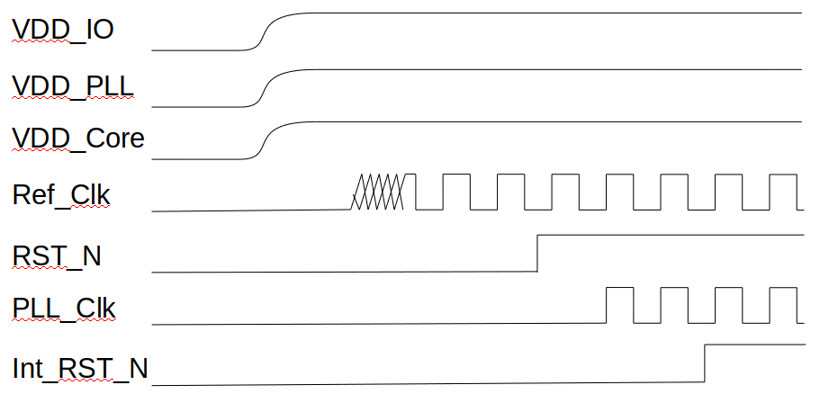
Reset
Reset is an active low input to the ASIC used to place the control logic into a known state.
The PLL reference clock should be operation for some period of time prior to flipping the reset pin.
Debug
Options
Clock mux, ability to use ref clk as internal clock
Clock out, send clock back out for analysis
Visbility mux, selected internal values muxed out for debugging
BIST
Registers
All programmer visible registers are described in this section.
Access | Meaning |
|---|---|
RO | Read Only |
WO | Write Only |
RW | Read and Write |
Register description tables use the following header:
Address (Hex) | Bit Fields | Description | Access |
MSU
Each MSU register addresses 64 bits of data. Multiple adjacent registers may be accessed in series by a single read/write command.
0x10 | 64 bits | Start Iteration | RW |
0x11 | 64 bits | Stop Iteration | RW |
0x12 | 64 bits | Intermediates Iteration | RW |
0x13-0x32 | 2048 bits | Initial value | RW |
0x33-0x53 | 2048 bits + 64 bits | Result buffer | RO |
Control Logic
Results Status and Control
0x0 | 0 – Result buf full 1 – Result buf empty 2 – MSU active 3 – Intermediates dropped 4 – Job queue full | Status | RO |
0x1 | 0 – Run 1 – Clear results 2 – Clear jobs | Control | WO |
0x2 | Debug mux configuration | RW |
IO Logic
IO Status and Control
Clock
0x | 0 – Lock enable 1 – Lock status (RO) | PLL Control/status | RW |
Core Clock Divider
Sets the clock divider for the desired core frequency.
0x | Core clock divider | RW |
Control Clock Divider
Sets the clock divider for the desired control logic frequency.
0x | Control clock divider | RW |
Thermal
ASIC Identification
On systems with multiple ASICs attached to a single host controller, there needs to be a mechanism to uniquely identify each device.
Pin List
The external pin list and package information is detailed in this section
Pin | Num | I/O | Description |
|---|---|---|---|
ref_clk | 1 | I | External reference clock for PLL |
SDA | 2 | I/O | I2C Data |
SCL | 3 | I/O | I2C Clock |
RST_N | 4 | I | Reset, active low |
VDD | X | I | Power (Do we need PLL, IO, and Core?) |
VSS | X | I | Power (GND) |
Therm_Trip | X | O | Thermal trip to cut off power on runaway temperature |
Debug | 5 | O | Debug internal signals |
System Level Operation
The ASIC is designed to operate in a variety of systems. There can be 1 to X ASICs per host controller in a single system.